
Critical Equipment Selection Factors in 60 Seconds
- Sub-7nm nodes require e-beam inspection (sub-10nm resolution) for critical layers; optical systems remain cost-effective for mature processes
- Hybrid strategies optimize total cost by deploying optical inspection for high-throughput non-critical layers and e-beam selectively
- Legacy platform uptime (2010-2018 vintage) depends on agile spare parts sourcing as traditional OEM support diminishes
- Total ownership costs include consumables, unplanned downtime, and emergency sourcing premiums over 10-15 year lifecycles
Critical Detection Challenges Across Fabrication Nodes
The transition to advanced process nodes fundamentally alters the defect detection equation. At geometries above 14nm, broadband optical inspection systems could reliably catch pattern fidelity issues and surface contamination. Field observations show this capability degrades sharply as feature sizes fall below 7nm. The physics are unforgiving: when critical dimensions become comparable to or smaller than the wavelength of the inspection light source, diffraction limits prevent reliable detection.
Advanced node economics demand dramatically tighter control—operational experience shows that even a handful of undetected defects across a 300mm wafer can destroy yield. The inspection system must combine high resolution with sufficient detection sensitivity to catch rare events without flagging excessive false positives that slow production throughput.
$8.9
billion
Global semiconductor metrology and inspection equipment market value in 2024, projected to reach $16.2 billion by 2033 driven by advanced node requirements
According to consolidated 2025 market data from Grand View Research, the global semiconductor metrology and inspection equipment market was valued at $8.9 billion in 2024 and is projected to grow to $16.2 billion by 2033. Since 2022, the CHIPS & Science Act has allocated over $100 million to advanced metrology research initiatives, addressing a critical infrastructure gap as fabs transition to advanced nodes.
Optical vs. Charged-Particle Inspection: Performance Trade-offs
Inspection technology selection hinges on matching detection capabilities to specific application requirements. The two dominant technology families—optical systems and charged-particle platforms—deliver fundamentally different performance profiles. As the 2024 IRDS Metrology roadmap from IEEE emphasizes, machine learning is becoming critical for real-time wafer inspection image analysis and reduced downtime in semiconductor production lines.
Broadband Optical Inspection Systems
Broadband optical platforms leverage visible and near-ultraviolet light sources to scan wafer surfaces at speeds exceeding 100 wafers per hour. This throughput advantage makes optical inspection the backbone of high-volume manufacturing. The technology performs reliably on layers where minimum feature sizes remain above approximately 20-30nm—covering mature node production (28nm and above) and non-critical layers in advanced node flows.
The limitation surfaces when feature sizes approach the inspection wavelength. Physics dictates that resolution limits prevent reliable detection of defects smaller than roughly half the wavelength of the light source used. For practical broadband optical systems, this translates to a detection floor around 10-15nm under optimal conditions.
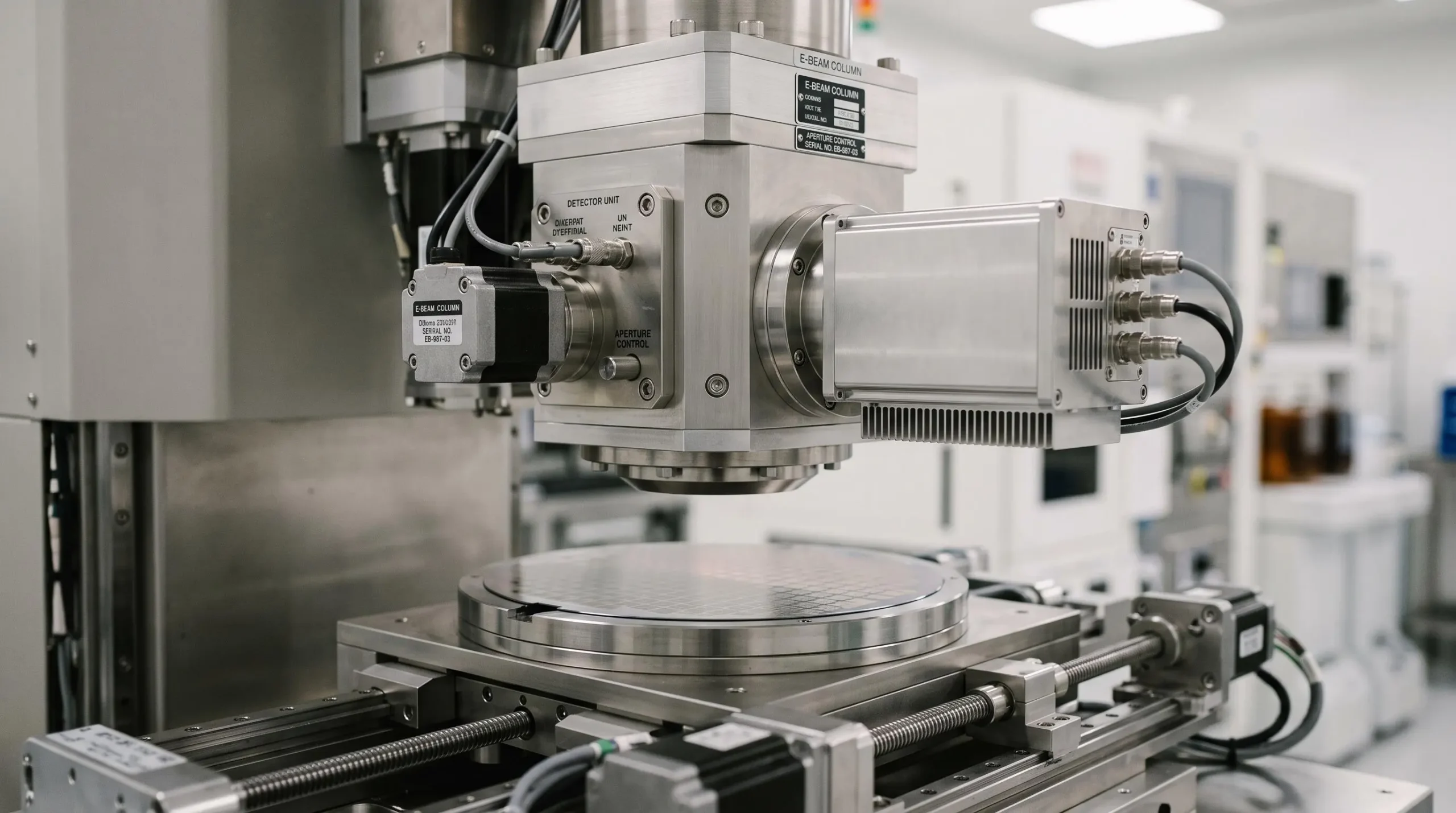
E-beam Defect Review and Inspection
Electron beam inspection systems achieve sub-10nm resolution by scanning wafer surfaces with a focused beam of electrons rather than photons. This charged-particle approach circumvents the wavelength-imposed resolution limits that constrain optical systems. The electron beam can be focused to spot sizes well below 5nm, enabling detection of defects at the most advanced production nodes (5nm, 3nm, and emerging 2nm processes).
E-beam platforms provide voltage contrast imaging—exploiting electrical properties of semiconductor structures to identify defects that affect conductivity or charge retention. The trade-off arrives in throughput: e-beam inspection operates at dramatically lower wafer processing rates, often measured in minutes per wafer rather than seconds. Equipment managers typically prioritize e-beam inspection for gate patterning, contact formation, and other critical process steps.
Emerging Hybrid Approaches
Industry consensus favors hybrid inspection strategies that combine optical and e-beam technologies. A representative approach might deploy broadband optical inspection as the primary screening method across all layers, with e-beam systems performing targeted inspection on the 10-15% of critical layers where advanced resolution is non-negotiable. This tiered strategy contains total capital expenditure while closing detection gaps at advanced nodes.
| Technology Type | Resolution Capability | Throughput | Optimal Application | TCO Consideration |
|---|---|---|---|---|
| Broadband Optical | Limited at sub-7nm nodes | High (100+ wafers/hour) | Mature nodes, non-critical layers, high-volume production | Lower CAPEX, higher throughput, moderate consumable costs |
| E-beam Inspection | Sub-10nm detection | Lower (targeting critical layers) | Advanced nodes (<7nm), critical dimension measurement, voltage contrast defects | Higher CAPEX, selective deployment reduces total cost vs full optical replacement |
| Hybrid Multi-Modal | Combines both approaches | Optimized by layer criticality | Mixed-node fabs, process transitions, cost-performance optimization | Strategic deployment minimizes over-investment while closing detection gaps |
Many production fabs operate mixed-node portfolios where mature processes (28nm, 40nm, or larger) still represent significant revenue. Wholesale replacement of functional optical inspection platforms with e-beam systems would constitute massive over-investment for layers where optical detection remains adequate. Understanding the importance of process monitoring across diverse manufacturing contexts helps clarify when technology transitions genuinely serve operational needs.
Sustaining Uptime in High-Volume Manufacturing Environments
Inspection equipment delivers value only when operational. According to SEMI E10 specification for equipment reliability, the industry maintains standardized methodologies for measuring RAM (Reliability, Availability, Maintainability) performance. High-volume fabs typically target uptime exceeding 98% for critical metrology and inspection platforms—a threshold that demands disciplined execution across three operational pillars: preventive maintenance, spare parts availability, and technical support responsiveness.
Preventive maintenance execution forms the foundation. Equipment managers who defer scheduled PM intervals inevitably pay the price through increased unplanned outages. This requires both organizational discipline and ready access to replacement components when PM schedules call for consumable refresh or wear part replacement.
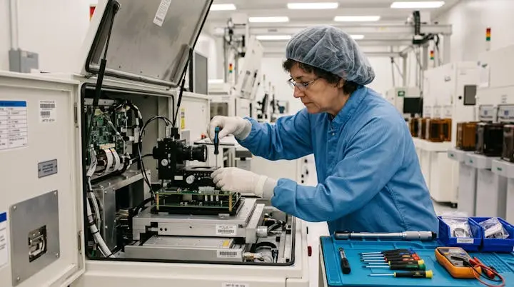
Spare parts availability presents particular challenges for legacy platforms still running production. Many fabs operate inspection equipment installed during the 2010-2018 era—systems that remain capable but increasingly difficult to support through traditional OEM channels. For KLA semiconductor platforms approaching end-of-life, alternative sourcing strategies that maintain strategic inventory of high-failure-rate components with 24-48 hour delivery timelines provide competitive advantage over OEM channels where lead times can extend to weeks. This agile approach to component sourcing directly impacts production continuity.
Maintaining Legacy Platforms: Three-Pillar Uptime Strategy
Equipment managers operating mixed-vintage inspection portfolios maintain uptime above 98% on legacy platforms through coordinated execution across three operational pillars:
Preventive Maintenance Discipline: Execute manufacturer-recommended PM schedules without deferral; track mean time between failures (MTBF) trends to anticipate component replacement before unplanned outages occur.
Agile Spare Parts Sourcing: Maintain strategic inventory of high-failure-rate components (valves, sensors, optical elements); establish relationships with suppliers offering 24-48 hour delivery for legacy platforms where OEM lead times extend to weeks.
Technical Support Access: Preserve internal expertise through documentation and cross-training as OEM field service availability declines; leverage third-party technical support for troubleshooting legacy configurations that original equipment manufacturers no longer prioritize.
Integrating Inspection Into Continuous Improvement Frameworks
Inspection data represents far more than a pass/fail gate in the production flow. Modern fabs integrate metrology and inspection results with upstream process equipment sensors to create closed-loop optimization mechanisms. When an inspection system flags a systematic defect pattern appearing at specific wafer locations, that spatial signature can correlate with process tool chamber conditions, consumable degradation, or recipe drift. This integration transforms inspection from reactive defect detection into proactive process control.
Statistical process control implementations leverage inspection data streams to track capability indices (Cpk) and detect process shifts before they exceed control limits. Early detection through trending of inspection results enables corrective action during routine maintenance windows rather than emergency interventions that disrupt production schedules. The most sophisticated implementations employ machine learning algorithms that analyze inspection images in real-time to identify subtle pattern anomalies that traditional rule-based classification might miss.
Equipment strategy ultimately serves a single objective: sustaining production continuity across technology transitions and equipment lifecycles. The balanced approach recognizes that equipment portfolios evolve incrementally rather than through complete generational replacements. A production line might operate 2015-vintage optical inspection tools on mature node layers, 2020-generation enhanced optical systems on intermediate nodes, and current e-beam platforms on the most advanced processes. This mixed vintage reflects rational capital allocation—deploying expensive cutting-edge technology only where its capabilities are genuinely required. Success depends on operational excellence: maintaining aging platforms through intelligent spare parts strategies as detailed in frameworks for quality assurance, executing preventive maintenance with discipline, and preserving the technical expertise required to troubleshoot legacy configurations.
- Audit current inspection capability against actual node requirements: identify layers where optical resolution remains adequate vs. critical layers requiring e-beam deployment
- Calculate total cost of ownership including spare parts, consumables, and unplanned downtime over remaining equipment lifecycle (not just initial CAPEX)
- Establish agile sourcing relationships for legacy platform spare parts before critical component failures force emergency procurement at premium pricing
- Verify internal expertise preservation for aging equipment: document configurations, cross-train technicians, reduce dependence on vanishing OEM field service
- Integrate inspection data with upstream process sensors to enable closed-loop optimization rather than treating metrology as isolated quality gate
The inspection equipment market’s projected growth to $16.2 billion by 2033 reflects the semiconductor industry’s ongoing technology intensity. As production transitions to 3nm, 2nm, and eventually sub-nanometer nodes, detection requirements will continue pushing technology boundaries. The operational challenge remains constant: deploying and sustaining the inspection capability required to maintain yield while managing the total cost of ownership across equipment lifecycles that span a decade or more.